Microstructuring of p-Si(100) by localized electrochemical polishing using patterned agarose as a stamp
ZHANG L, ZHUANG J-L, MA X-Z, et al.
Microstructuring of p-Si(100) by localized electrochemical polishing using patterned agarose as a stamp [J]. Electrochemistry Communications, 2007, 9(10): 2529-33.

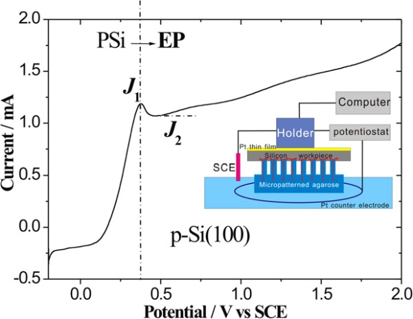
Fig. 1. Typical current–voltage curve for a p-Si(100) electrode placed on a micropatterned gel soaked in 0.6 mol/L HF. At potential lower than Upeak = 0.39 V, porous Si (PSi) is formed on the electrode. For Usi > Upeak, the Si electrode dissolves in the electropolishing regime (EP). The insert is a schematic drawing of the experimental set-up specially designed for electrochemical polishing.

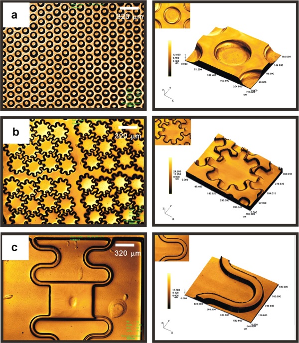
Fig. 2. (a) Micrographs of a fabricated micro-hole array and the 3D structure of a single hole, (b) micrographs of a fabricated micro-gear array and the 3D structure of a single gear and (c) micrographs of curvilinear ridges and the 3D structure of a single ridge with a sharp edge.

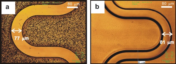
Fig. 3. (a) Micrograph of the curvilinear ridge on a master of Si and (b) microstructure fabricated on p-Si in 0.8 mol/L HF with an etching time of 4 h.
文章链接:http://www.sciencedirect.com/science/article/pii/S1388248107003219