Micromachining on copper and nickel by electrochemical wet stamping
TANG J, ET AL.
Micromachining on copper and nickel by electrochemical wet stamping [J]. Journal of Micromechanics and Microengineering, 2010, 20(11): 115030.

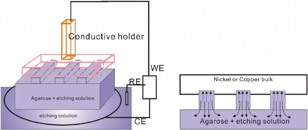
Figure 1. (a) Schematic illustration of the setup used in the E-WETS technique. (b) Detailed illustration of the diffusion path of the solution(solid line) and that of the product (dashed line).

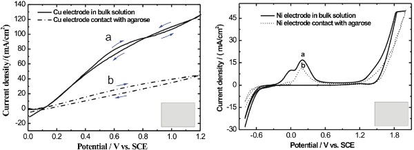
Figure 2. (a) Cyclic voltammogram of a Ni electrode in a 1.0 M H3PO4+0.85 M Na2SO4 solution (solid line) and placed on a micropatterned agarose stamp soaked in the solution (dashed line). Scan rate: 50 mV s−1. (b) Cyclic voltammogram of a Cu electrode in 0.1 M HClO4 (solid line) and placed on a micropatterned agarose stamp soaked in 0.1 M HClO4 (dashed line). Scan rate: 50 mV s−1.

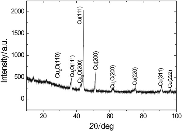
Figure 3. Glancing angle x-ray diffraction scan of the thin film formed on the copper surface. Glancing angle = 1?.

Figure 4. (a), (b) Microscope images of curvilinear ridges on Cu and (c) microscope images of a concave gear wheel array fabricated in a solution of 0.1 M HClO4. The potential was 0.4 V versus SCE and the machining times were 3600 s and 2400 s, respectively. (b) The zoomed image of (a). The inserted image of (b) is the curvilinear ridge on a master of Si.

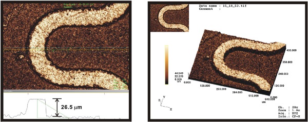
Figure 5. The section analysis of the microstructure on Cu and the 3D structure of the etched Cu ridge.

Figure 6. (a), (b) Microscope images of curvilinear ridges on Ni and (c) microscope images of a concave gear wheel array fabricated in a solution of 8% H3PO4+12% Na2SO4+2% glycerin+1% sodium tartrate for 30 min with pulse amplitude, duration and interval 8 V, 0.001 s and 0.002 s, respectively. (b) The zoomed image of (a). The inserted image of (b) is the curvilinear ridge on a master of Si.
文章链接:http://iopscience.iop.org/0960-1317/20/11/115030/